Lasers
AUTOMATED TECHNOLOGICAL MACHINE BASED «Karavella» on copper vapour laser
Application: precision treatment of sheet materials (0.05…0.6 mm)
Spectrum of treatable materials:
- refractory metals (W, Mo, Ta) and their alloys
- high thermoconductive metals (Cu, Ag, Al, Au) and their alloys
- steels and other metals
- semiconductors and dielectrics
- polycrystalline diamonds
- transparent materials
Available operations:
- precision outline cutting
- microhole drilling
- scribing
- modification of near-surface layer
- formation of images within of transparent media
Machine configuration
- Copper vapour laser (CVL) “Kulon-15”, made as “oscillator-amplifier” pattern
- PC-based travel and control system
- Optical system of delivering and focusing the beam in the treatment zone
- Technological chamber
- System of gas supply into the treatment zone
- System for destruction products removing from the treatment zone
- Carrier structure
Advantages Technological:
- Contactless treatment
- Small size of the processing spot (10…40 ?m)
- Evaporative nature of treatment (minimum liquid phase)
- Low roughness of the cutting edge (? 1…3 ?m)
- Low thermal effect area (? 5…10 ?m)
- High precision of treatment (4…20 ?m)
- No splitting or chipping of materials
- Higher productivity (Vtr=1…10 mm/s)
Structural:
- Simple beam power control system
- Laser system of observation using the amplifier active element
- High repeatability and stability of the active element parameters
- Long service life and possibility of express active elements replacement
- Simple adjustment of the machine
The advantages are provided by the following factors:
- Sealed-off design of CVL active elements
- Laser power supply with a switching element based on IJBT-transistors
- A long-term experience in the fields of CVL application in the material precision treatment technology.
Potential industrial applications
- Electronic industry: fabrication of grids, electrodes, other vacuum device parts, heatsinks, synthetic diamond elements, separation of substrates.
- Instrument engineering: production of diaphragms, matrixes and structural elements, tool marking
- Automobile industry: production of engine injectors and heat duty sensors.
- Chemical industry: production of spinnerets; tonal marking of products.
- Medical industry: filters, catheters, probes, artery expanders.
- Jewelry industry: precious material cutting, and treatment, manufacture of souvenirs, 3D-marking of glass and others.
| Radiation wavelength, nm | 510,6 и 578,2 |
| Radiation beam diameter, mm | 14 |
| Average radiation power, W | 10…15 |
| Pulse repetition frequency, kHz | 13…14 |
| Pulse width (on level 0,5), ns | 10±1 |
| Average radiation power variation at steady operation(within 8 hour of monitoring), % | 5 |
| Radiation pulse energy, mJ | 0,1…1 |
| Beam divergence, mrad | 0,1…0,3 |
| Focusing length, mm | 50,70,100,150,200 |
| Heel radiations diameter in planes of the processing, ?m | 10…40 |
| Coordinate table travel on XY plane, mm | 150х150 |
| Coordinate table travel along vertical axis Z, mm | 60 |
| Coordinate table travel rate, mm/s | 20 |
| Positioning error of each axis at (20±1)?C, ?m | ± 2 |
| Magnification of laser tracking system | 300 |
| Operation readiness time, min | 60 |
| Continuous operation time, hours | unlimited |
| 3-phase network power consumption, kW | 5 |
| Water consumption | (water-water or water-air system ) |
| Overall dimensions and location area, mm and m2 | 3000х1700х1350; 7 |
| Weight, kg | 1150 |
| MTTF, hours | 1500 |
| Average recovery time after active element replacement, hours | 3 |
Results of precision treatment:

A part of spherical grid from molybdenum (МЧ), 0,07 mm thick

Grooves in tungsten (W) 0,2 mm thick

Polycristal diamond cut 0,35 mm thick
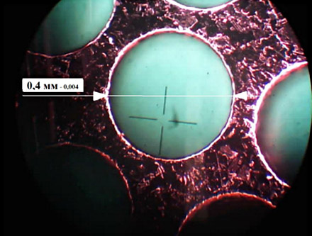
Holes in cuprum (МВ) 0,3 mm thick
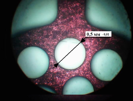
Holes in pseudoalloy (МД-80) 0,6 mm thick
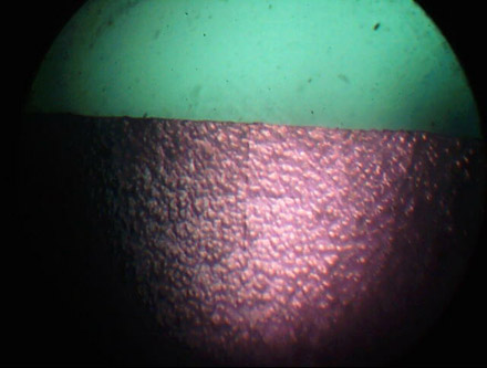
Silicon (Si) cut 1 mm thick
AWARDS
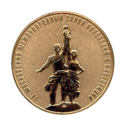
1. Gold medal at IV Moscow the International Interior of innovations and investments (February, 2004)
2. Gold medal at 53-rd World Interior of innovations, scientific researches and new technologies Brussels-Eureka 2004» (November 2004)
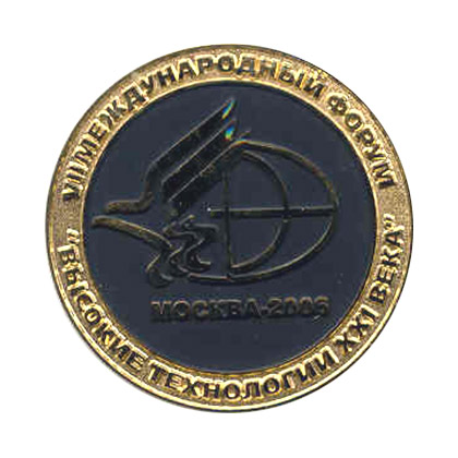
3. Gold medal at VII International Forum «High technologies of XXI century» (April 2006)